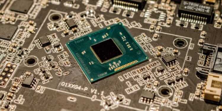
The Bhabha Atomic Research Centre (BARC) is offering technology for producing high purity copper oxide nano particles (CuO NP) from used, waste printed circuit boards.
The technology involves hydrometallurgical route using novel polymeric resin. The process begins with generation of acidic leach liquor of copper from printed circuit boards (PCBs), followed by feed acidity adjustment for removal of tin and selective uptake of copper using novel copper selective resin. After scrubbing under optimized conditions, high purity copper is obtained by elution with mild acid in continuous column mode. Copper is then precipitated and calcined at high temperature to yield high purity CuO nanoparticles. Further, using same resin, lead is recovered from the raffinate of leach liquor and subsequently converted into commercially valuable lead sulfide. The process therefore offers fully scalable technology for production of CuO nano particles, SnO and PbS from e-waste. This process promises abundant profit and employment opportunity to the electronic waste recycling industry, and offers long term solution for sustainable electronic waste management.
Although base metal copper and copper oxide (CuO) has low commercial value, CuO nanoparticles have immense commercial value and unique applications. The process developed is for specifically enabling environmentally concerned metal recyclers to achieve scaled-up production of high purity copper oxide nanoparticles in continuous mode operation from waste PCBs. The major steps are leaching, selective metal sorption/desorption by functionalized polymeric resins, precipitation and filtration of the product for final drying and packaging of CuO nanoparticles along with PbS and Sn-oxide as by-products. All the unit operations are easily scalable and the necessary process equipments are commercially available and are not capital intensive. Technology for synthesis of Cu-selective resin is also given along with the process.
This technology thus provides the advantage of commercially producing very high purity metal compounds right from e-scrap, thus providing considerable financial gains at the same time mitigating the environmental concerns of ever increasing e-waste, transforming it into a valuable resource for making the country technologically self-reliant.
Salient features
- A process for production of copper oxide nano particles (purity >99.9%) from printed circuit boards (PCBs)/powder concentrate, using indigeneously developed polymeric resin.
- Such a process is developed for the first time wherein, one of the potentially hazardous waste (e-waste) is processed to produce highly techno-commercial and anti-viral product (copper oxide nano particles).
Advantages
This technology empowers metal recyclers to start production of high purity copper oxide nanoparticles which has immense techno-commercial value. This process also ensures toxic ‘lead’ free effluent discharge from PCBs processing, hence making e-waste recycling both commercially profitable as well as environmentally friendly.
Uses
Copper oxide nanoparticles are applied in electronics Manufacturing, sensors and solar cells, anti-microbial and anti-fouling coatings, electrochemical energy storage, heterogeneous catalysis and rocket propulsion.
Facilities required
- Depopulating unit: For making bare PCB boards free of other components
- Delamination unit: Removal of polymer layer over PCB board for effective leaching
- Leaching unit: Leach reactor with agitator, electricity and water supply, Nutsche filter for separation of leach liquor and storage leach liquor, HCl handling and storage and feed preparation tank
- Metal sorption/desorption unit: Novel Cu-selective resins, Cylindical Acrylic columns for holding polymeric resins, pumps with flow control, suitable piping, electricity and water supply, eluent preparation and storage tank
- Precipitation unit: Reactor with agitator for precipitation of copper compound from loaded eluent and filtration using Nutsche filter
- Heating Furnace: Product drying, conversion to oxide
- Packaging unit: For packing products CuO NPs, PbS and SnO powders
- Analytical facility: For analysis of Cu, impurities like Pb and Sn, pH etc.
- Demineralization/decontamination unit: Ion-exchange unit for recycling/disposal of process water after removal of ions.
- Ventilation system: For handling HCl fumes generated during leaching
- Electrical Supply: Required for running of various process equipment
- Chemical Storage Unit: Stocking of raw materials needed for different unit operations
- Facility for synthesis of Cu-selective resin
For further details, contact:
Head, Technology Transfer and Collaboration Division
Bhabha Atomic Research Centre,
Trombay, Mumbai 400 085.
Fax :+91-22- 25505151
technology@barc.gov.in
ALSO READ:
IIT Bombay technology for new material for carbon capture
Novel composite material for high temperature batteries and super capacitors
High performance thermoelectric material


